Simplify Your Printed Circuit Board Making
Simplify Your Printed Circuit Board Making
There are many different types of Printed Circuit Board materials in the market these days. The common ones are FR-1, FR-2, CEM-1, CEM-3 and FR-4 . The thickness of the PCB can be 1.0mm,1.2mm or 1.6mm. They can be single sided or double sided with cooper clad of 1 oz or 2 oz.
These are the common low cost PCB that eletronics hobbyist or students can use for their projects. Of course there are more complicated multilayer PCB that are used in the industry for various applications.
 | PCB Design Solution The most affordable PCB solution program in the industry. Freeware version available for evaluation. |
If you are an electronics hobbyist or students who are tight on the budget of making Printed Circuit Board, how do you make your own printed circuit board? If you were like me, I used to go through the many processes in making the PCB a few years ago. I used to make the PCB layout, print the layout on a suitable transparency (one that can withstand the temperature of the laser printer and photocopy machines), use of photoresist chemical (require a dark room to do this) on the PCB to ensure that the PCB pattern can be transferred to the PCB, transfer the layout from the transparency to the PCB by the use of ultra violet light, use of developer to develop the pattern on the PCB, etched the developed pattern on the PCB, washed the PCB, drilled the required holes, mount the components and solder the components.
Over the years, I have found out that with the advancement of technology, there are better ways to do the Printed Circuit Board processes. It helps to eliminate the use of darkrooms, photoresist chemical, developer chemical, negatives/transparency, ultra violet lights and long waiting time to cure the photoresist.
In simplifying the making of PCB, the direct benefit of this is it reduces the cost needed to set up the PCB making facilities.
The items below are the simplified steps of making simple single sided or double sided PCB for electronics hobbyists, students, or even electronics designer.
PCB Layouts Software
 |
There are many different types of PCB Layouts software and tools in the market these days. If you are a student or an electronics bhobbyist that are tight on budget, the information here will help you get some freeware or demo version with minimal functions for your projects.
You will be able to find some low cost softwares as well. For most electronics hobbyist or student, one does not need to have a complicated and features rich software tools. All you need is some basic features that enable you to create some simple single-sided or double-sided layouts.
You have to look out for two types of software design. One is the schematic entry software where you create a schematic diagram of your electronic circuit. This software usually has libraries of schematic such as transistor, resistor, capacitor, integrated circuits, microprocessor, micro controllers, connectors, LEDs, diodes and other standard components. If the component you use is not available, you are also allow to create your own and add it to the library.
The other software is printed circuit layout software where you import the schematic entry diagram and use it to draw the circuit. This layout is then used printed out and together with the data used to produce the PCB.
EAGLE
This CAD software for PCB schematic and PCB routing is easy to use. You can donwload free evaluation version to try out. You can also sign up for free webminar offered by CADSOFT which are offered in English, German, French and Spanish. Topics available include basics of the software, multilayer board design and generating manufacturing data.
PCB Design Rule Simplified
 | There are a few things to look out for when one does the PCB layouts. It is important to take note that the layout must take into consideration the cost factor as well as the practicality of making the PCB in-house. Listed below are some of the design rule that one should try to adhere while doing the PCB layouts. The detailed EMC(Electromagnetic compatibility) aspects will not be covered here. |
The followings are the suggested PCB design rule that one should try to adhere to in order to minimise the cost of fabricating the PCB. This design rule is specifically done for electronicsenthusiasts as well as students who are still not familiar with the fundamentals of PCB design and layouts.
a) Single Sided PCB and PCB material
As far as possible, one should try to layout the PCB to single sided layer as far as possible.It may be quite difficult to rout the PCB but with the use of jumpers, you should be able torout most of the simple circuity into single sided PCB. Of course at times you may need to usedouble sided PCB and multilayer PCB. The use of double sided PCB will increase the price to 1.5 to 2.5 times compared to single sided PCB. Common single sided PCB thickness is 1.6mm, 1 oz cooper clad, CEM-1 or FR-2 materials. As far as possible, try to use FR-2 which is paper phenolic type of PCB material. This is by far among the cheapest PCB that is used in most consumer electronics products today.
b) Panelisation of PCB
The PCB laminates normally comes in standard sizes. One of the common PCB laminates come in dimension of 40 inches X 48 inches. In order to maximise the use of the PCB, you should findout from the manufacturers the standard PCB sizes that they are using. By effective panelisationof the PCB, you can use up to 80%-90% of the PCB laminates. This will reduce the cost of eachPCB. If the layout panelisation is not effective, wastage up to 50% may occurred. Therefore,always check the effective panelisation of PCB before sending for fabrication.
If you are doing the prototyping yourself, this PCB Design Rule applies as well.
c) Size of the PCB
You should try to make use of the smallest area of the PCB as possible taking into considerationthe track width, spacing and other constraints. Always try to minimise the size of PCB duringthe layout of the PCB. The size of the PCB is critical being the fundamental of the PCB DesignRule.
d) Reduce the number of holes and vias
Whether you send the PCB for CNC (computer controlled PCB drilling) or you drill the holes yourself, you should try to reduce the number of holes and vias on the PCB. Since the timeutilised by the machine will determine the price of the PCB, the lesser holes and vias willreduce the cost of the PCB. The rule is to keep it simple and as basic as possible.
e) Reduce the number of types of holes sizes
Try to design with common hole size as much as possible. This is to avoid changing the drill bitsused by the machine. By having many types of hole sizes, the machine will have to change the drill bits and this takes time. The time taken will determine the cost of the PCB. Common drillbits sizes are 0.7mm, 0.8mm, 0.9mm, 1.0mm, 1.2mm, 1.5mm, 2.0mm and 3.0mm.
f) Track Width and track spacing
For your own prototying or even sending out for PCB houses for fabrication of the PCB, it is always advisable not to design the track width and track spacing to the limit of the manufacturercapabilities. For instance, if you need to design 0.3mm track width, try to use 0.5mm. Similarlyif the minimum track spacing needed is 0.3mmm, use 0.5mm instead. This will help to ensure thatthe yield is high during the production of the PCB.This PCB Design Rule is especially critical if you are fabricating the PCB on your own.
g) Silkscreen minimisation
If top overlay silkscreen is required, the PCB Design Rule recommend that you do not need to silkscreen the bottom overlay. It may be difficult to do trouble shooting later on but eliminating this process will save some cost as well.
PCB Design Layout Rules Recommendation
 | In the PCB design of electronics circuit, it is important that one plan and has a checklist of the do's and don'ts before proceeding to do the printed circuit board layout. The understanding of the circuit is critical to the design, for example one needs to understand the maximum current and voltage that are carried by each conductor in order to determine the track width of the conductor and the type of PCB that will be used. Some examples of the IPC standard are provided here. |
PCB Design Layout
In the PCB design of electronics circuit, it is important that one plan and has a checklist of the do's and don'ts before proceeding to do the printed circuit board layout. The understanding of the circuit is critical to the design, for example one needs to understand the maximum current and voltage that are carried by each conductor in order to determine the track width of the conductor and the type of PCB that will be used.
The voltage difference between each track will determine the clearance between each conductor. If the clearance is not enough, chances are that the electrical potential between each track will cause spark over and short circuit the PCB. This will cause functional failure to the product and the safety of the users that are using the product will be compromised. It is therefore critical for one to understand some of this basics requirements before one proceed to design the PCB.
Tracks Restricted Area
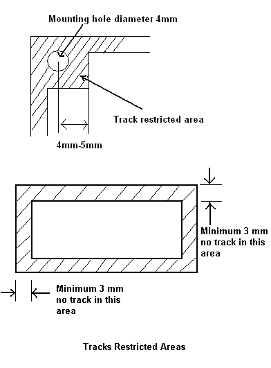
Tracks should not be located on the areas that can caused them to be peeled off easily. One of the restricted area is holes on the PCB which are used to mount screws or PCB spacers. These holes are usually used to secure the PCB to a casing or to secure it in a fixed place.
The edges of the PCB should not have any tracks as these areas are usually used to transport the PCB from one process to another process by using a conveyor belt. These edges are places where the possibility of scratches and cracking of the PCB happens. The recommended areas that should not have any track is as shown in the diagram below assuming a hole diameter of 4 mm which is used to mount a PCB spacer.

Conductor Thickness and Width
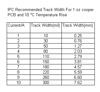
The PCB conductor thickness and width will determine the current carrying capacity of the track. The IPC standard for the conductor thickness and width of the common 1 oz/square-feet PCB is as shown below. However, it is always advisable to use a bigger value due to the tolerance and variation of the PCB processes. If higher current carrying capacity is required, a 2 oz/square-feet or 3 oz/square-feet type of PCB is preferred. Many electronics hobbyist prefer to solder a thick cooper conductor on the PCB track to increase the current carrying capacity of the track.

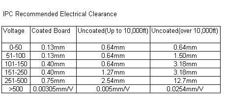
PCB Design Electrical Clearance Many safety standards call for a minimum of 8mm clearance between 240V mains and other isolated signal tracks. These safetystandards are to ensure that the users that are using the products will be protected from any electrical hazards.
For non main voltages, IPC recommend the electrical clearance between adjacent tracks. It is important to know the maximum difference in voltage that are applied on the adjacent tracks of a PCB. The electrical clearance specs of IPC standard is as shown below for various condition of the PCB. Coating the PCB will help to reduce the requirements of the track clearance. However, the quality of the coating as well as the material used are critical to ensure that these requirements are met. Again, it is always advisable to increase the clearance to cater for the variations of the PCB processes.

PCB Prototypes in Minutes
 | Once the PCB layout has been completed, one can start thinking of transferring the layout from the CAD software or even the layout from electronics magazines. The author would like to suggestthat one jump over the steps of using transparency, photoresist chemical, developer chemical andthe use of Ultra Violet light. The use of Printed Circuit Board Transfer Film will eliminatesthe steps mentioned. If your layout is in the CAD software, just print the layout onto this transfer file using a laser printer. If your layout is in the form of hardcopy like magazines orartwork, all you need to do is to photocopy the layout into the PCB transfer Film. |
As the technology advancement in PCB Prototypes and Protyping becoming more in the last few years, the old methods of using photoresist, developer and ultra violet light has been now confined to massproduction of PCB. Electronics hobbyists and students will definitely welcome the use of PCBtransfer film in the making of simple PCB Prototypes.
There are many companies that are supplying this film, but the author's favorite is using Press-n-Peel from Techniks Inc, New Jersey.
In a few short steps you can produce your own PCB Prototypes in minutes using Press-n-Peel PCBTransfer Film. Press-n-Peel offers you the ability to take magazine or computer generated pcb layouts, and either photocopy or laser print them onto the Press-n-Peel Film, and subsequently transfer that image onto copper clad printed circuit board material by using an iron. Peel offthe layer and etch the board in ferric chloride and you have a high quality pc board in minutes.
The steps below illustrates the simplicity of this PCB Prototypes method.
1) Photocopy or Laser Print circuit image onto the dull side (emulsion) of Press-n-Peel Image Transfer Film.
Prepare: Clothes Iron, Steel Wool #00 (or SOS/Brillo with all the soap washed out), Packaging Tape,Photocopy or Laser Printed Circuit Image.
2) Cut Press-n-Peel, leaving a 1/4" border around the circuit image. Cut board to size.Clean copper board with steel wool, S.O.S. or Brillo pads. Rinse cleaned board with soap and water. Be sure to remove all soap residue. Dry thoroughly with lint-free cloth. Be sure to scrape any burrs that appear on the edge of the board that may have resulted from the cutting/shearing process. Burrs tend to keep the iron from making solid contact with thePress-n-Peel Film
3) Place Press-n-Peel with image face down onto clean copper board. Iron the Press-n-Peel Filmto the board a peice of plain paper between the iron and the film to reduce friction. Temperature setting on the iron is critical, and dependant upon your laser printer or photocopier. Suggested starting temperature is 275-325 degrees F. Iron setting is generally "polyester". Iron temperatures vary. Iron until board has completely and fully reached thetemperature of the iron. Time varies with the size and thickness of the board. Generally this is 1.5 to 10 min. DO NOT USE THE STEAM SETTING!
4) Quench the board/film combination under cold running water. Peel the film off.To remove small "fills" in between traces and "filled donuts", cover the imaged copper board with clear packing tape, and then remove. This will pull all unwanted filled areasoff the board.
5) After removing "fills", trim the board (if necessary) to the final size. Wash the board in soap & water before etching to remove surface oxidation . Etch with Ferric Chloride (Note: Techniks does not sell PCB etching supplies -- available through local electronic supply stores & Radio Shack)
6) Using steel wool, scrub the Press-n-Peel image off as to reveal copper traces. This is best done under running water. Suggestion: Do not do this until your ready to drill and populatethe board. The Press-n-Peel transfer resist protects the board from oxidation.
Detailed diagram with instructions can be obtained from the following
Press-n-Peel PCB Prototypes link.

Comments
Post a Comment